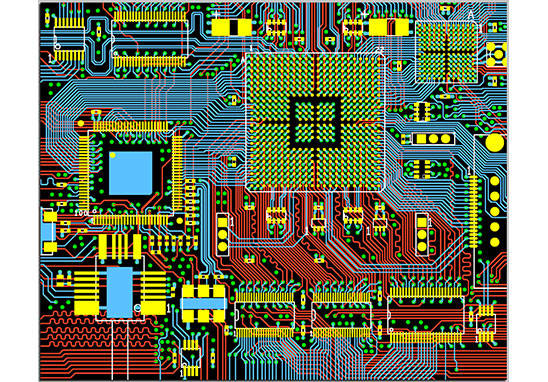
PCB design component layout principles
1. The components should be arranged inside the PCB board, and each lead-out of the component should occupy a separate pad.
2. The components cannot occupy the entire PCB panel, and a margin of 5~10mm must be left around the board. The size of the PCB board area and the fixing method determine the size of the margin around the board.

4. The installation height of the components should be as low as possible. If it is too high, it is easy to fall over or touch adjacent components, which may cause the safety performance of the system to deteriorate.
5. What determines the axial position of larger components is the installation state of the printed circuit board in the system. The axial direction of the regularly arranged components should be in the vertical direction in the system, thereby improving the stability of the components on the PCB board. sex.
6. The span at both ends of the component should be slightly larger than the axial length of the component. When bending the pins, do not bend them all at once, leave a distance of about 2mm to avoid damaging the components.
7. The layout of components should not cross up and down, and a certain distance should be maintained between adjacent components, and the spacing should not be too small.


